
480-858-0393
orders@mspecllc.com
Specialties LLC. 1815 W 1st Ave,
ST 112 Mesa, AZ 85202
Monday - Friday 07h - 22h
Closed on Weekends

Test Boards
Test boards from M Specialties LLC Specialties are made using the latest proven design techniques and materials. They are designed to meet the ever growing demands for higher speeds – reduce signal reflections, cross talk, and noise for applications into the Giga-Hertz range.
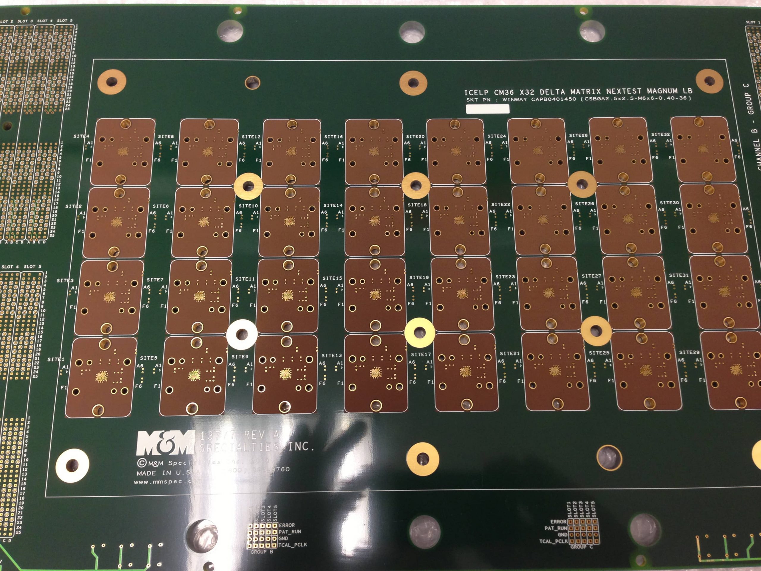
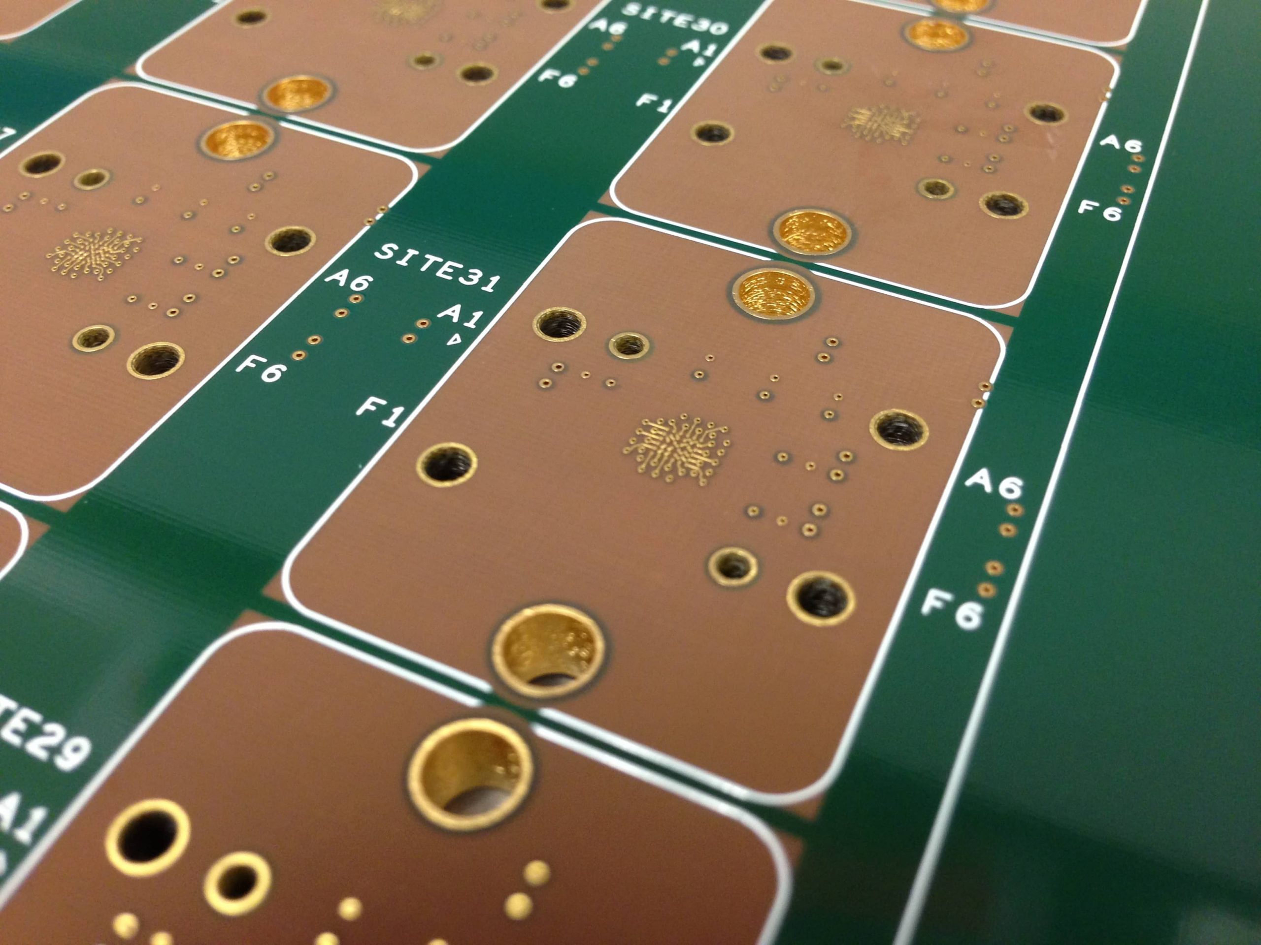
ATE BOARDS
(Application specific Load boards and Probe cards)
| Advantest | Teradyne | LTX/Credence | Verigy (Agilent) | Others | |
|---|---|---|---|---|---|
| 1 | T5334 | CATALYST | Diamond Series | 82000 Series | MCT 2000 |
| 2 | T5381 | INTEGRAFLEX | LT1101 | 83000 Series | MCT 3100 |
| 3 | T3340 | MICROFLEX | LT1001 | 93000 Series | Mosaid 3495 |
| 4 | T5581 | TIGER | VISTALOGIC | 93000 PINSCALE | Mosaid 4105 |
| 5 | T5591 | ULTRAFLEX | VISTAVISION | 93000 W/RF PORT | Sentry Series |
| 6 | T3381 | A500 SERIES | Vanguard | 9400 Series | |
| 7 | T5335 | J937 | Quartet | 95000 Series | |
| 8 | T5592 | J750 | Octet | VERSATEST 3300 | |
| 9 | T5593 | J971 | SC212/312 | ||
| 10 | J973 | ASL1000/3000 | |||
| 11 | J993/5/7 | ||||
| 12 | J994 | Fusion Series | |||
| 13 | J996 | Deltta Master | |||
| 14 | Synch Master | ||||
| 15 | Array Master | ||||
| 16 | Delta 50 |
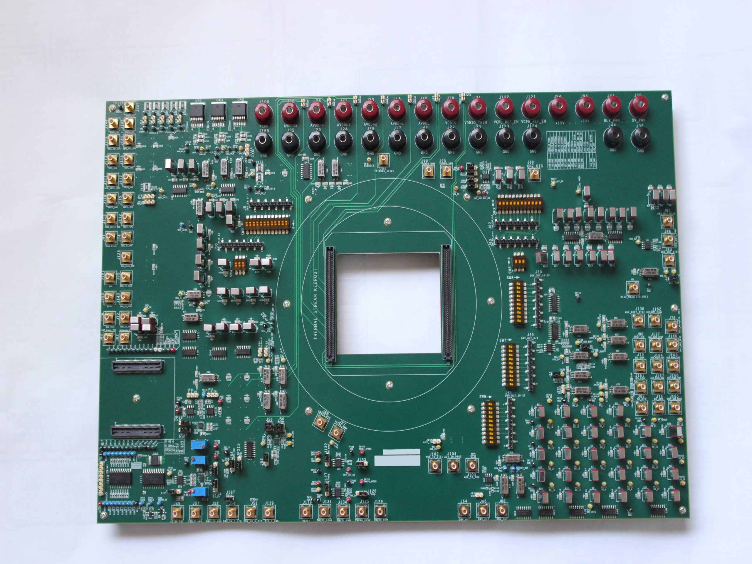
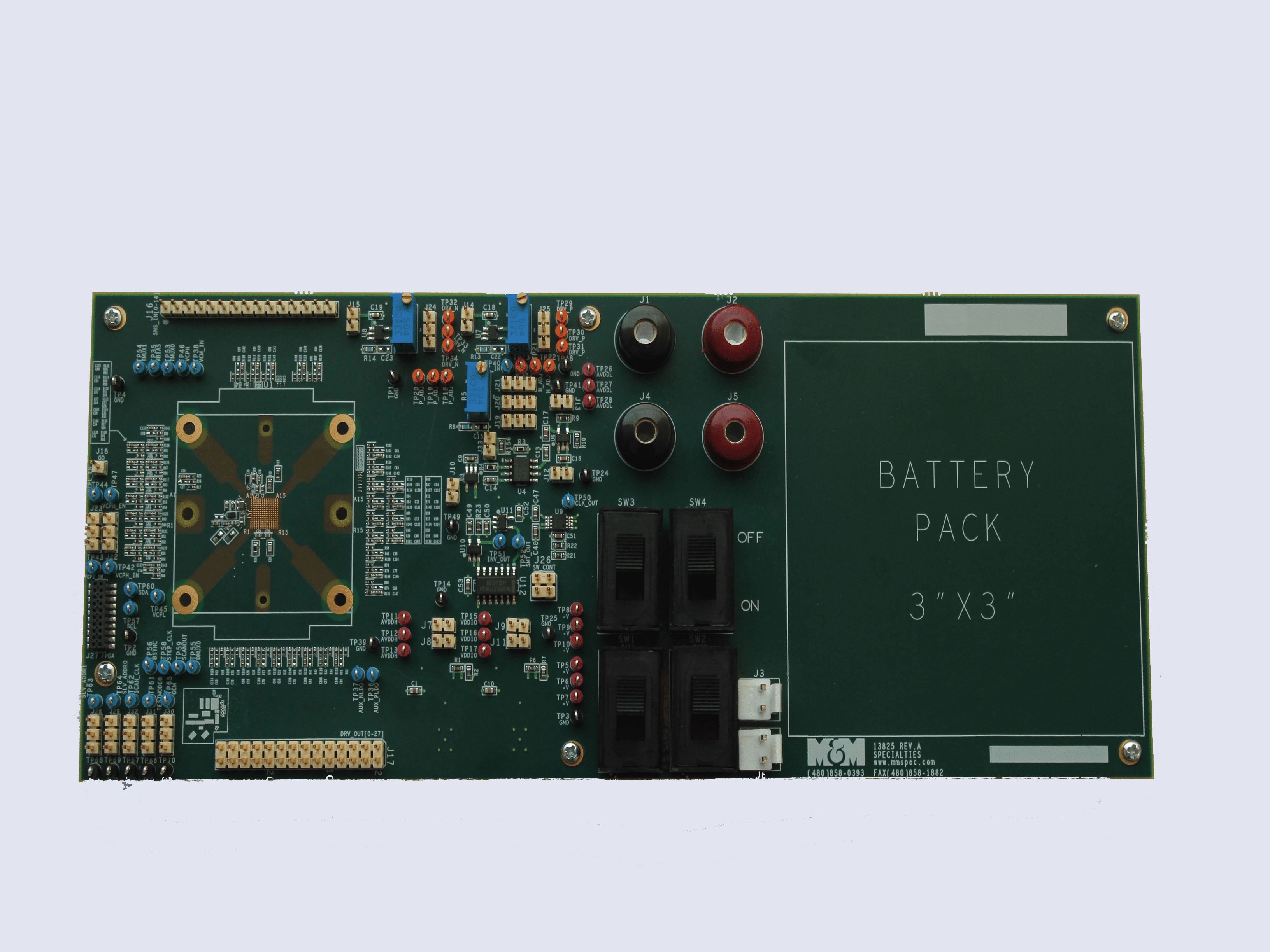
PCB Design
M Specialties LLC’s experience in the design and manufacturing of printed circuit boards is unmatched by anyone in the industry. Our years of experience includes work with mixed signal, high speed digital and RF applications. We design our boards to be 100% compliant with each tester manufacturer guidelines. We create all of our templates from the Tester manufacturers specifications, and have compiled a wide variety of templates over the last 35 years.
When it comes to manufacturing boards, we use only qualified partners who deliver quality products on time; while utilizing the best materials and practices.
We are committed to meeting your requirements at every stage of the process; from characterization to production.
SOFTWARE
We use the latest CAD software tools such as Cadence Allegro and Mentor PowerPCB to design and layout our boards.
Design & Layout
Cadence Allegro
Mentor Graphics Powerpcb
Schematic Entry
Orcad
Concept HDL
Power Logic
DESIGN AND RF SIMULATION CAPABILITIES
.003 trace widths with .003 drill to trace spacing
Pin to pin spacing as low as .4mm on multi-site designs.
Experience with drill aspect ratio >30:1
Experience using Blind, Buried and back drills to alleviate stubs
Stacked Vias using HDI technology with 4 lamination cycles.
Conductive filled vias down to .4mm spacing
4% impedance tolerance available upon request
Experience with 44 layers at .290″ thickness
Proper selection of dielectric material (ex. Fr-4, Nelco, Rogers, GeTeK etc.).
Ansoft HFSS, Sigrity and Hyperlynx with IBIS and HSPICE models
Return loss and Insertion Loss simulation
EMC/EMI analysis.
Eye Diagrams for critical nets.
Crosstalk analysis
Via impedance measurement.
Pre and Post Layout measurements.
Decoupling solution for PDN.
MANUFACTURING CAPABILITIES
use of only qualified PCB manufacturing partners.
100% matching of LVS and Gerbers using IPC netlist.
2 Phase QC process to verify DRC and DFM.
Experience with most advanced materials (Arlon, Nelco, Rogers, Getek, etc.).
Complete TDR report to show controlled impedance matching.
ASSEMBLY CAPABILITIES
Full Pick & Place, Re-flow
Use in house and also qualified Assembly house with full testing capabilities.
3-D xray capabilities
Huge Library with trusted Footprints of discretes and ICs with our own p/n.
Fully automated BOM and Assembly drawing.
In house inventory of frequently used parts & components.